As a strategic emerging industry, semiconductor lighting is one of the important ways for China to develop its low-carbon economy and adjust its industrial structure and green development. During the "12th Five-Year Plan" period, the 863 Program for New Materials Technology supported the major project of "R & D of key material technologies for efficient semiconductor lighting". Recently, 863 plan office of new material technology in Beijing organized experts to the project acceptance. The project of "Research and Development of Key Materials for High Efficiency Semiconductor Lighting (Phase I) and Phase II (Phase II)" carried out researches on LED epitaxy and industrialization key technologies of high luminous efficiency and low cost, and chip and package application technologies on Si and sapphire substrates. Developed high-quality SiC and GaN substrates, deep UV LED devices, high-efficiency white OLED devices and lamps, high-quality GaN epitaxial materials, high-power LED film flip-chip devices and other achievements, access to independent intellectual property rights with high-quality white lighting products , The localization of key materials such as high purity metal organic compound (MO) source, phosphor, silica gel and so on, and the application of LED in the field of plant growth and medical treatment have been realized. During the "Thirteenth Five-Year Plan" period, in order to speed up the scientific and technological innovation and industrialization in the field of materials, the Ministry of Science and Technology formulated the "Special Plan for Scientific and Technological Innovation in the Field of Materials in the 13th Five-Year Plan", focusing on the development of new materials and technologies , Advanced structure and composite materials, new functions and smart materials to meet the development needs of strategic emerging industries. In the direction of the development of strategic electronic materials, the third-generation semiconductor materials and semiconductor lighting technology are systematically distributed. The key research contents include: regulation of epitaxial growth of large-sized, high-quality third-generation semiconductor substrates and thin film materials, efficient full spectrum Light Sources Core Materials, Devices and Lamps Full Technology Chain Green Manufacturing Technologies, Beyond Lighting and Visible Light Communication Key Technologies, System Integration and Application Demonstration, High Performance RF Devices, Power Electronics and Modules Design, Process Technology and Application Demonstration, Core Equipment Manufacturing Technology and so on.
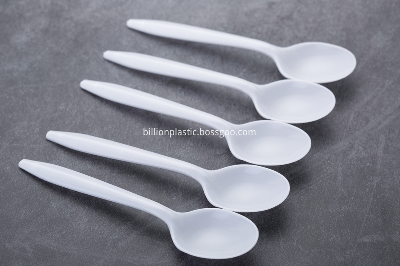
Produce by Food Grade PP material, this PP spoon is a good solution for eating various dishes without getting hands involved . Its usability: Airline catering, food courts, hotels, parties, fast food and Ice cream outlets, coffee shops,picnic, outdoor events and all types of catering houses.
Plastic Spoon ,Disposable PP Cutlery,PP Disposable Spoon,Disposable Plastic Cutlery,Disposable Spoon,Reusable Plastic Spoons BILLION PLASTIC MANUFACTURING CO.,LTD, JIANGMEN , https://www.jmfoodpackagingbag.com

Breakthrough was made in the major project of R & D of key materials for highly efficient semiconductor lighting